
 Tiếng Việt
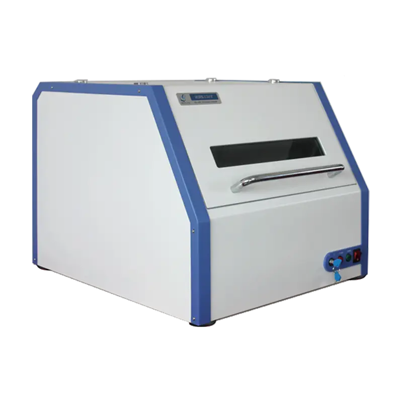
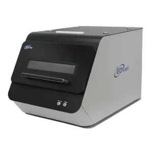
iEDX-150T Coating Thickness Gauge
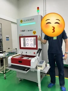
Explore the authentic iEDX-150T coating thickness gauge at Maxlab Equipment. This XRF device features a 125eV SDD detector, isolating up to 5 plating layers and measuring alloy ratios automatically without sample destruction, delivering high precision for the PCB and electronics industries.
Product Information
Transforming Quality Control Processes with the iEDX-150T Coating Thickness Gauge
In today’s high-tech industrial supply chains, particularly in printed circuit board (PCB) manufacturing, semiconductor production, and precision engineering, the surface plating layer plays a critical role in determining a product’s lifespan, electrical conductivity, and corrosion resistance. A plating layer that is too thin leaves components vulnerable to peeling and oxidation; conversely, an excessively thick layer—especially when using precious metals like Gold, Silver, or Palladium—unnecessarily drives up production costs.
To solve this stringent quality control challenge, Maxlab Equipment introduces a cutting-edge technological solution to the market: the iEDX-150T. This next-generation coating thickness gauge utilizes energy-dispersive X-ray fluorescence (ED-XRF) technology and is developed and manufactured by Sense (SANS Instrument).
1. Current Challenges in Surface Plating Thickness Inspection
Within factory QA/QC departments, verifying the thickness of a plating layer after it emerges from the electrolyte bath often encounters major bottlenecks when using traditional methods:
- Destructive Testing (Metallographic Cross-Sectioning): Engineers must cut the product in half, embed it in resin, polish it, and then examine it under a microscope to measure the thickness. While accurate, this method completely destroys the finished product, causing significant waste for expensive components and consuming a vast amount of time.
- Conventional Handheld Gauges: These devices can only measure simple, single plating layers over magnetic metal substrates. When faced with complex multi-layer structures or alloy plating systems, these tools are completely ineffective or yield massive errors due to background noise interference.
- Errors Caused by Changing Plating Formulas: Every time a workshop adjusts its chemical composition ratios or switches to a new plating system, recalibrating legacy measurement machines is a complicated task that requires purchasing expensive standard foils from overseas.
2. iEDX-150T – The Pinnacle of Non-Destructive Multi-Layer Analysis Technology
Distributed officially by Maxlab Equipment, the iEDX-150T model offers a perfect synergy of robust hardware and intelligent spectrum-processing algorithms, enabling factories to fully automate their surface quality evaluation processes.
Superior Hardware Configuration
The heart of the iEDX-150T coating thickness gauge is its premium Silicon Drift Detector (SDD), which delivers an ultra-high energy resolution of 125 ± 5 eV.
In the micro-world of electronic plating, metals such as Iron (Fe), Cobalt (Co), Nickel (Ni), and Copper (Cu) exhibit fluorescence energy levels that sit extremely close to one another on the periodic table. Armed with a 125eV resolution, the iEDX-150T operates like an ultra-fine mesh filter, precisely isolating the characteristic spectral lines of each element and completely eliminating spectral overlapping or noise interference from the underlying base metal.
Capacity to Isolate Up to 5 Overlapping Plating Layers
The iEDX-150T boasts incredible analytical capability, measuring and simultaneously bóc tách (deconvoluting) up to 5 plating layers stacked on a single surface in just one scan (for example, a highly complex system like Gold / Palladium / Nickel / Copper over a Steel substrate). The machine displays the detailed thickness of each individual layer with a refined display resolution down to 0.001 μm (1 nanometer) in just 10 to 30 seconds.
3. Exclusive Features Positioning the iEDX-150T Above the Rest
Simultaneous Measurement of Thickness and Alloy % Ratio
This is a strategic, game-changing feature of the iEDX-150T. In modern industrial plating systems such as Nickel-Phosphorus (Ni-P) or Zinc-Nickel (Zn-Ni), the quality of the coating is governed not only by its thickness but also by the weight percentage ratio (%) of its constituent elements.
- For instance: A Zn-Ni plating layer must maintain a specific ratio of 12% to 15% Nickel relative to the total mass of the plating layer to ensure optimal corrosion resistance.
The iEDX-150T leverages the intelligent Fundamental Parameter (FP) mathematical algorithm to calculate the reverse absorption of X-rays within the material matrix. Consequently, with just a single click, the machine yields both the exact thickness in micrometers and the alloy percentage ratio instantly, without destroying or scratching the product.
Automated 3D Sample Stage (XYZ Auto Stage)
To optimize productivity for busy QC departments, the iEDX-150T comes equipped with a three-dimensional (XYZ) automated sample stage controlled directly via its software. Combined with a 2.0 MP high-definition positioning camera, engineers can map out specific measurement points across a PCB. The machine then automatically navigates, engages its auto-focus, and fires X-rays at multiple consecutive positions to verify plating uniformity across the entire component surface.
Flexible Standardless Calibration
Thanks to the FP algorithm, which comes pre-loaded with a library of universal physical constants, when a factory modifies its electroplating formula, engineers simply update the coating structure diagram in the software. The system automatically recalculates the absorption matrix without forcing the user to own expensive physical standard foils to set up a new baseline from scratch, translating to maximum long-term operational savings for the business.
4. Practical Applications in Spearhead Industries
The elemental analysis range of the machine extends from Aluminum (Al) to Uranium (U), allowing the iEDX-150T to perfectly cater to multiple factory segments:
- Electronics & PCB Manufacturing: Measures ultra-thin plating thicknesses such as Electroless Nickel Immersion Gold (ENIG), ENEPIG, and Tin (Sn) plating on contact pins and flexible circuit boards.
- Automotive & Aerospace Industries: Monitors the quality of heavy-duty anti-corrosion layers like Zinc-Nickel (Zn-Ni) alloy plating and hard Chromium plating on piston rods, structural bolts, and heavy-wear fasteners.
- RoHS Screening: The machine integrates a rapid scanning feature to screen and alert users to the presence of hazardous substances banned under European standards (such as Lead – Pb, Mercury – Hg, Cadmium – Cd) within component coatings prior to export.
5. Comprehensive Technical Services from Maxlab Equipment
By choosing to acquire the high-end iEDX-150T from Maxlab Equipment, customers receive more than just high-quality hardware; it comes wrapped in a professional after-sales technical ecosystem:
- Tailored Installation and Calibration: Maxlab’s engineers visit the factory to configure exclusive, optimized Calibration Curves, neutralizing matrix errors based on the customer’s actual substrate materials and plating solutions.
- In-Depth Technology Transfer: Thorough training is provided to QC engineers on how to program the automated stage, read spectra, and analyze plating flaws based on energy graphs.
- 24/7 Technical Support: We commit to rapid on-site warranty, maintenance, and troubleshooting to ensure that the factory’s continuous production chain remains uninterrupted.
The iEDX-150T coating thickness gauge is a smart strategic investment that helps enterprises solidify their quality reputation with major international partners, minimize defect rates, and thoroughly optimize precious raw material costs. Contact Maxlab Equipment today for an in-depth consultation and a tailormade commercial quotation.