

 Tiếng Việt
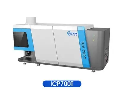
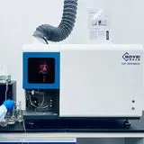

ICP-700T Inductively Coupled Plasma Emission Spectrometer
Explore everything about the inductively coupled plasma emission spectrometer (ICP-OES). Discover its working principle, exceptional technical advantages, and practical applications in trace element analysis.
Product Information
Inductively Coupled Plasma Emission Spectrometer: The Ultimate Lab Solution
In the era of high-tech industrial manufacturing, accurately determining the chemical composition of materials plays a decisive role in both product quality and environmental safety. To meet strict analytical standards at the micro and trace levels, the inductively coupled plasma emission spectrometer (commonly referred to as ICP-OES or ICP-AES) has become an indispensable analytical instrument in modern laboratories worldwide. This article provides a comprehensive analysis of the working principle, outstanding technical features, and practical applications of this high-end analytical equipment.
1. What Is an Inductively Coupled Plasma Emission Spectrometer?
An inductively coupled plasma emission spectrometer is an advanced physicochemical analysis device that utilizes plasma energy excited by a high-frequency radio frequency (RF) source to atomize and excite elements within a sample, causing them to emit light. By measuring the specific wavelengths of this emitted light and their corresponding intensities, the device enables laboratory technicians to qualitatively and quantitatively determine dozens of chemical elements simultaneously with extreme precision.
2. The Fundamental Working Principle
The analytical procedure of this sophisticated instrument undergoes four strict and automated steps:
- Sample Vaporization: The liquid sample is drawn by a precise peristaltic pump into a nebulizer, where it is transformed into a fine aerosol (a mist of tiny droplets).
- Plasma Excitation: These fine aerosol particles are carried directly into the core of an Argon gas plasma torch. This plasma environment reaches ultra-high temperatures ranging from 6,000°K to 10,000°K.
- Optical Emission: At this extreme temperature, all chemical bonds within the sample are broken down, transforming the sample into excited free atoms or ions. As these unstable particles return to their lower energy or ground state, they release energy in the form of optical radiation (light spectrum). This emitted light features unique, characteristic wavelengths for each specific chemical element.
- Detection and Processing: The internal optical system collects the emitted light, separates it into monochromatic wavelengths using high-resolution gratings, and directs it onto a sensitive detector (such as a photomultiplier tube – PMT, or solid-state sensors like CCD/CID). The software then calculates the exact concentration based on the intensity of the light.
3. Outstanding Technical Advantages of the Equipment
Compared to traditional atomic spectroscopy methods such as AAS (Atomic Absorption Spectroscopy), the inductively coupled plasma emission spectrometer possesses several superior technical characteristics that make it a preferred choice for high-throughput labs:
- Simultaneous Multi-Element Analysis: The instrument can scan and identify over 70 elements (including almost all metals and several non-metals) in a single run. This drastically reduces analysis time and optimizes laboratory operational efficiency.
- Ultra-Low Detection Limits and Sensitivity: Thanks to the high energy of the plasma torch, the system achieves detection limits down to the parts-per-billion (ppb) level. This capability allows the precise tracking of trace elements and ultra-small impurities that other devices might miss.
- Wide Linear Dynamic Range: The device can directly measure samples with concentrations spanning 5 to 6 orders of magnitude. This means it can measure both ultra-low trace amounts and high-concentration elements simultaneously without requiring tedious, multi-step sample dilutions.
- High System Stability: Modern systems incorporate a solid-state RF generator with automatic frequency matching. This design ensures that the plasma flame remains perfectly stable under varying sample matrices and heavy organic workloads.
4. Diverse Real-World Applications
Due to its exceptional analytical capabilities, this equipment is widely deployed across a variety of vital industrial sectors:
- Environmental Monitoring: It is used to measure toxic heavy metals (such as lead, cadmium, arsenic, and mercury) in industrial wastewater, drinking water supplies, municipal soils, and agricultural sediments.
- Geology and Mining: The system assists in determining precious metal concentrations in mineral ores, analyzing the matrix composition of rocks, and precisely separating rare earth elements used in semiconductor manufacturing.
- Metallurgy and Material Science: Laboratories utilize the device to inspect the purity of raw metals, verify the exact components of high-end alloys, and maintain strict quality control in silicon wafer production.
- Petrochemical and Chemical Industries: It plays a crucial role in analyzing trace element contaminants in crude oil, evaluating wear metals in engine lubricants, and certifying petrochemical derivatives to prevent machinery degradation.
In conclusion, the inductively coupled plasma emission spectrometer serves as a vital tool that enables enterprises, universities, and research institutions to master material analysis. Investing in this technology enhances analytical capability, optimizes manufacturing quality, and ensures full compliance with international technical and safety standards.
Be the first to review “ICP-700T Inductively Coupled Plasma Emission Spectrometer”
Related products
ANALYSIS INSTRUMENT
ANALYSIS INSTRUMENT

ANALYSIS INSTRUMENT

ANALYSIS INSTRUMENT

ANALYSIS INSTRUMENT

ANALYSIS INSTRUMENT

ANALYSIS INSTRUMENT
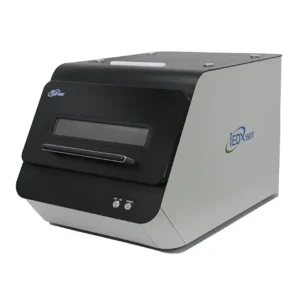
iEDX-150µT – X-Ray Plating Thickness Gauge Ultra-Thin Coatings

ANALYSIS INSTRUMENT





Reviews
There are no reviews yet.