

 Tiếng Việt
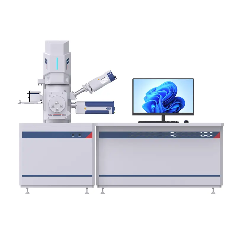
BestScope BSEM-691 scanning electron microscope
Discover the genuine BestScope BSEM-691 scanning electron microscope at Maxlab Equipment. The article analyzes technical specifications, outstanding features, and the BSEM-691LV low vacuum variant for effective non-conductive sample analysis.
Product Information
The BestScope BSEM-691 scanning electron microscope is an advanced material surface analysis solution, delivering outstanding performance for modern laboratories. Distributed officially by Maxlab Equipment, this model combines high-durability tungsten filament technology with an optimized electron optical lens system. This is the premier choice for applications in materials science research, semiconductor component quality inspection, geology, and forensic science.
Overview of BSEM-691 Scanning Electron Microscope Technology
The equipment utilizes a traditional tungsten filament electron source but has been powerfully upgraded in terms of its vacuum chamber and focusing system. This structure ensures that the emitted electron beam achieves high stability, minimizes noise, and significantly extends the lifespan of the filament. Consequently, the operational and routine maintenance costs of the machine are substantially lower than those of more complex field emission systems.
Featuring a large sample chamber design and a 5-axis automated movement stage, users can easily manipulate various specimen shapes and sizes. The intuitive control software interface maximally assists technicians in optimizing images, performing micro-scale measurements, and exporting data rapidly.
Impressive Features and Technical Specifications
The BSEM-691 model possesses robust technical specifications, meeting strict standards in microstructure analysis:
- Optimal Resolution: The device achieves an image resolution of up to 3nm at an accelerating voltage of 30kV when using the secondary electron (SE) detector. For the backscattered electron (BSE) detector, the resolution reaches 4nm, allowing for clear observation of ultra-fine details on the sample surface.
- Flexible Magnification Range: The microscope supports magnification from 1x up to 300,000x, enabling users to easily switch from macro-overview observation to detailed analysis of nanostructure regions.
- Customizable Accelerating Voltage: The voltage range extends from 0.2kV to 30kV, allowing flexible adjustment depending on the sensitivity of the specimen to the electron beam, thereby minimizing charging effects or sample damage.
- Powerful Integration Capability: The sample chamber is pre-designed with more than 10 expansion ports, ready for upgrades to connect with energy-dispersive X-ray spectroscopy (EDS), wavelength-dispersive X-ray spectroscopy (WDS), or electron backscatter diffraction (EBSD) systems to analyze quantitative chemical composition and crystal structures.
BSEM-691LV Low Vacuum Variant: A Solution for Non-Conductive Samples
One of the outstanding advantages of this product line is the existence of the BSEM-691LV (low vacuum) variant. For conventional scanning electron microscopes operating in a high vacuum environment, non-conductive specimens such as polymers, ceramics, paper, textiles, or biological samples easily accumulate electrical charges on their surfaces. This causes image blurring and distorts the observation results. To overcome this, users are forced to perform an extra step of coating a thin layer of gold or carbon onto the sample surface.
The BSEM-691LV variant completely resolves this difficulty thanks to its flexible pressure control capability within the sample chamber. The low vacuum mode allows a small amount of gas to be introduced into the chamber. These gas molecules are ionized by the electron beam and neutralize the negative charges accumulating on the surface of the non-conductive specimen. Users of the BSEM-691LV can place dry biological samples, organic materials, or electrical insulators directly into the chamber for immediate observation without undergoing complex preparation steps or applying conductive coatings. This not only saves chemical costs and preparation time but also perfectly preserves the natural structure of the sample.
Practical Applications and Benefits of Choosing Maxlab Equipment
The BestScope BSEM-691 microscope is widely applied in analyzing surface morphology, measuring particle sizes, inspecting weld defects, and evaluating thin film quality. When choosing this product from Maxlab Equipment, customers are guaranteed professional service quality. This includes transportation, anti-vibration platform installation, optical system calibration, and comprehensive technology transfer training from a team of highly experienced engineers.
Be the first to review “BestScope BSEM-691 scanning electron microscope”
Related products
MICROSCOPE
Industrial Inspection Microscope
Stereo Microscope
Biological Microscope
Portable Microscope
BPM-620/BPM-620M BestScope Portable Metallurgical Microscope







Reviews
There are no reviews yet.